Move over Graphene: Next-Gen 2D Materials Could Revolutionize Technology – Discover Magazine
The wonder material graphene — an array of interlinked carbon atoms arranged in a sheet just one atom thick — promised a world of applications, including super-fast electronics, ultra-sensitive sensors and incredibly durable materials. After a few false starts, that promise is close to realization. And a suite of other extremely thin substances is following in its wake.
Graphene got its beginnings in 2003, when scientists at the University of Manchester found they could peel off a gossamer film of the material just by touching a piece of ordinary sticky tape to a block of purified graphite — the solid form of carbon that’s mixed with clay and used as the “lead” in most pencils. Graphene proved stronger than steel but extremely flexible, and electrons could zip through it at high speeds. It earned its discoverers the Nobel Prize in 2010, but researchers spent years struggling to manufacture it on larger scales and figuring out how its remarkable properties could best be used.
They didn’t get it right straight out of the gate, says Todd Krauss, a chemist at the University of Rochester. “Scientists are pretty bad at predicting what’s going to be useful in applications,” he says.
With its atom-thin sheets layered into tiny particles known as quantum dots, graphene was tried as a microscopic medical sensor, but it didn’t perform as desired, Krauss says. With its sheets rolled up into straw-like nanotubes, graphene was built into items like hockey sticks and baseball bats in the hopes that its strength and durability could better existing carbon fiber. But Krauss notes that there has since been a trend away from using nanotubes in consumer products. (Some also worry that long carbon nanotubes could harm the lungs since they have been shown to have some chemical resemblance to asbestos.)
Today graphene is finding its way into different types of products. “Graphene is here,” says Mark Hersam of Northwestern University. Layered over zinc, graphene oxide is actively being developed as a replacement, with higher storage capacity, for the sometimes unreliable graphite now used in battery anodes. And nanotubes were recently used as transistors to build a microprocessor, replacing silicon (unlike flat graphene, nanotubes can be coaxed into acting like a semiconductor). Though the microprocessor was primitive by modern computing standards, akin to the processing level of a Sega Genesis, materials scientists think it could ultimately pave the way for more efficient, faster and smaller carbon components for computer processors.
At the same time, a new generation of two-dimensional materials is emerging. The success of graphene further fueled the ongoing effort to find useful atomically thin materials, working with a range of different chemicals, so as to exploit the physical properties that emerge in such super-thin substances. The newcomers include an insulator more efficient than conventional ones at stopping the movement of electrons, and another that allows electrons to glide across it at a good percent of the speed of light, with little friction. Researchers think some of these may one day replace silicon in computer chips, among other potential uses.
Other materials now in development have even higher aspirations, such as advancing scientists toward one of the most tantalizing goals in chemistry — the creation of high-temperature superconductors.
In graphene, carbon atoms link up in an orderly honeycomb pattern, each atom sharing electrons with three neighboring carbon atoms. That structure allows any added electrons to move speedily across its surface. Ordinarily, a single electron might move through a conducting metal like copper at 1.2 inches per minute (given a 12-gauge wire with 10 amps of electricity). But in early experiments on graphene, electrons zipped along at 2.34 billion inches per minute — which could make for electronics that charge in just a few minutes and eventually in a matter of seconds.
Graphene’s physical properties have inspired many potential applications, including in medicine. A variant of graphene, graphene oxide, is being studied as an experimental drug delivery vehicle. Seen here through a microscope, this chunk of graphene oxide is about 80 nanometers high. A single sheet of graphene is just 0.34 nanometers thick.
Graphene conducts heat just as well as it conducts electricity. It’s also one of the strongest materials ever studied — stronger than steel, it can stop a bullet — but oddly stretchy too, meaning it’s both flexible and tough.
Other 2D materials under exploration may have similar attributes as well as novel qualities all their own, but chemical impurities have until recently kept them hidden, says Angela Hight Walker, a project leader at the National Institute of Standards and Technology in Gaithersburg, Maryland. “We’re now getting to the point where we can see the new physics that’s been covered up by poor sample quality,” she says.
One of the newcomers is black phosphorus, explored by Hersam and his coauthor Vinod Sangwan in the 2018 Annual Review of Physical Chemistry. When white phosphorus — a caustic, highly reactive chemical — is super-heated under high pressure, it becomes a flaky, conductive material with graphite-like behavior. Peeling off an atom-thin layer of this black phosphorus with sticky tape produces a material called phosphorene. First fabricated in 2014, phosphorene rivals graphene in terms of strength and ability to efficiently move electrons. But at the atomic level, it isn’t as perfectly flat as graphene — and that has intriguing consequences.
Phosphorene interacts with electrons and photons in quirky ways, pointing to potential uses in future computer chips and fiber optics.
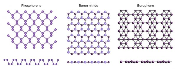
In graphene, carbon atoms lie side by side, hence its flatness. But phosphorene’s 2D configuration looks a bit like a pleat, with two atoms at a lower level connected to two at a higher level, forming what’s called a bandgap. This wavy structure, in turn, affects the flow of electrons in a way that makes phosphorene a “semiconductor,” meaning that it’s very easy to switch the flow of electrons on or off. Phosphorene, like silicon, could find application in computer chips, where the toggled electrons represent 1s or 0s.
Phosphorene also is especially good at emitting or absorbing photons at infrared wavelengths. This optical trick gives phosphorene huge potential for use in fiber-optic communication, Hersam says, because the bandgap matches the energy of infrared light near-exactly. It could also prove very useful in solar cells.
Working with phosphorene is not easy, however. It is highly unstable and rapidly oxidizes unless stored correctly. “Literally, it will decompose if it is sitting out in the room,” Hight Walker says, typically in less than a minute. Layering it with other 2D materials could help protect the fragile chemical.
Boron would seem an odd fit for electronic applications. It’s better known as a fertilizer, an ingredient in fiberglass or (combined with salt) a laundry-detergent additive. But make it very thin and very flat, and boron begins to act more like a metal, conducting electricity easily. Two-dimensional boron, called borophene, is also ultra-flexible and transparent. Combined with its conductive properties, borophene’s flexibility and transparency could eventually make it a go-to material for new gadgets, including ultra-thin, foldable touch screens.
Like graphene, borophene’s structure allows electrons to fly through it. It’s such a good conductor that it’s now being studied as a way to boost energy storage in lithium-ion batteries. Some researchers even think it might be coaxed into superconducting states at relatively high temperatures — though that’s still very cold (initial tests show the effect between minus-415 to minus-425 degrees Fahrenheit). Most current superconductors work close to absolute zero, or nearly minus -460 degrees F. A superconducting material allows electrons to move through it without any resistance, creating the potential for a device that accomplishes robust electronic feats while using only a small amount of power.

Emerging 2D materials phosphorene, borophene and boron nitride form thin films. Their atomic arrangements are viewed here from above and in profile. (Credit: Modified from V.K. Sangwan and M.C. Hersam/AR Physical Chemistry 2018)
In the form of borophene, boron can conduct electrons like a metal. Yet, as part of a 2D-film of boron nitride, it can block the flow of electrons quite effectively. “In other words, 2D boron and [2D] boron nitride are on opposite ends of the electrical conductivity spectrum,” Hersam says.
Boron nitride’s insulative property has come in handy for research on other 2D materials. Take that ephemeral black phosphorus: One way scientists have managed to keep it stable enough to study is by sandwiching it between two sheets of boron nitride.
Even as it is blocking electrons, however, boron nitride will allow photons to pass, says physicist Milos Toth of the University of Technology Sydney, who coauthored an article about the potential of boron nitride, and other 2D materials, in the 2019 Annual Review of Physical Chemistry. That’s ideal for creating things called single-photon sources, which can emit a single particle of light at a time and are used in quantum computing, quantum information processing and physics experiments.
Another atomically thin material creating quite a buzz in materials science circles is a compound of chromium and iodine called chromium triiodide. It’s the first 2D material that naturally generates a magnetic field. Scientists working on chromium triiodide propose the material could eventually find uses in computer memory and storage, as well as in more research-focused purposes such as controlling how an electron spins.
There’s a hitch, Hersam says: “This material is extremely hard to work with,” because it is both tough to synthesize and unstable once it’s made. Right now the only way to work with it is at extremely low temperatures, at minus-375 degrees Fahrenheit and below. But boron nitride might again come to the rescue: Some chromium triiodide samples have been preserved for months on end inside boron nitride sandwiches.
Because of its finicky properties, chromium triiodide may not itself end up built into devices, Hight Walker says. “But when we understand the physics of what’s happening, we can go look for this 2D magnetic behavior in other materials.” A number of 2D magnetic materials are now being explored — single-layer manganese crystals woven into an insulating material is one possibility.
Wrangling any of these thin layers into something usable may ultimately depend — literally — on how they stack up. Different super-thin materials would be layered together so that the properties inherent in each material can complement one another. “We have insulators, semiconductors, metals and now magnets,” Hight Walker says. “Those are the pieces that you need to make almost anything you want.”
One potential application especially exciting to Hight Walker is in quantum computing. Unlike traditional computing, in which bits of information are either ones or zeroes, quantum computing allows each “qubit” of information to be both one and zero at once. In principle, this would allow quantum computers to quickly solve problems that would take an impossibly long time with conventional machines.
Right now, though, most qubits are made of superconductors that have to be kept freezing cold, limiting their real-world use and motivating the search for new types of superconducting materials. For this reason, researchers are eager to explore borophene’s ability to superconduct. (Graphene, layered a certain way, also has shown potential superconducting properties.)
But a stacked material involving several superconducting layers separated by strong insulators could enable smaller, more stable qubits that don’t require quite as low temperatures — which could reduce the overall size of quantum computers. Right now, these are room-sized affairs, much like early computers were. Reducing their size is going to require novel approaches and, possibly, very thin materials — layered sheet by little sheet.
10.1146/knowable-112219-1
John Wenz is digital producer at Knowable Magazine. His first book, The Lost Planets: Peter van de Kamp and the Vanishing Exoplanets around Barnard’s Star, came out October 2019 from MIT Press.
This article originally appeared in Knowable Magazine, an independent journalistic endeavor from Annual Reviews.


